Flexible PCBs for IoT
The IoT ecosystem has evolved at a rapid pace. The proliferation of connected devices has made it essential to develop smaller, more durable circuit boards that can accommodate the varying shapes and sizes of these devices. This is where flexible PCBs come in. These circuits are pliable enough to bend to conform to a device’s form factor and provide excellent electrical performance, reduced volume and weight, and higher copper tensile strength, making them ideal for IoT devices.
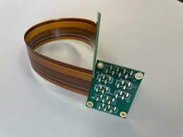
The simplest type of flexible pcb is called a single-sided flex circuit and has a conductive copper layer on one side of the dielectric material, usually polyimide or a polymer film. A metalized hole connects the two copper sides to complete the circuit. This is a common configuration for wearables and small embedded/IoT devices. More advanced flexible circuits use a double-sided flex board that has a conductive copper layer on both sides of the dielectric material. A pair of metalized holes connect the two copper sides to complete the circuit.
For complex, high-speed applications, a multi-layer, rigid-flex PCB may be needed. A rigid-flex circuit combines the flexibility of a flex circuit with the rigidity of a standard printed circuit board to ensure good conductivity, signal integrity, and signal timing. It is an excellent solution for high-density, high-speed applications that require the conductive paths to be routed in a tight space.
When designing a flex circuit, you must consider the flexing characteristics and maximum available bend radius of the board in addition to its thickness, layout, and component placement. This will help you determine the best fabrication process for your circuit.
Flexible PCBs for IoT Devices
Once you have finalized your design and arranged the traces, holes, and labels, you can begin the layout process with your PCB software. This step includes routing the traces, adding reference designators, and making any other changes required by your layout. Once the layout is finished, your PCB files will be ready for the fabrication and assembly process.
The fabricator will use a precise laser to bore tiny holes in the flex substrate, then fill them with copper using the through-hole plating procedure. Once the copper is plated, the flex substrate goes through a blanking process, which cuts it into the correct sizes using either a hydraulic punch or kick the bucket set.
Once the flex PCB is in its final form, it will undergo an electrical testing and inspection process to make sure that all the components are functioning properly. The inspection also helps to detect any flaws in the flex circuit that might affect its functionality.
When considering the use of flexible PCBs for your IoT project, it’s important to consult with a trusted PCB manufacturer. They can advise you on the best options for your specific application and provide a free quote. To learn more, contact a PCB manufacturer today.