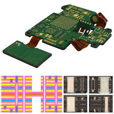
Design Flex Circuit Boards
When you design a flex circuit board, you need to consider the operating environment. This can be as simple as whether the product will be static or dynamic. If the product will flex back and forth continuously, then the flex circuit board needs to have a specific level of flexibility that can accommodate this movement. Otherwise, it will be very difficult to install the PCB within the device.
You also need to decide on a flex substrate material. These are typically polyester or polyimide films. Conductive material traces are then etched on the flex substrate and covered with a layer of protective coverlay. You can choose between a variety of adhesives, including acrylic, epoxy, and pressure-sensitive (PSA) adhesive films. The choice depends on the specific application and what will be the most cost-effective.
In addition, you will need to determine what type of copper is appropriate for your flex circuit board. ED copper is plated and is prone to work hardening and fatigue. Rolled annealed copper is a better option, as it has a higher strain tolerance and can bend without fracturing.

How to Design Flex Circuit Boards
Once you have a good idea of your operating environment, it’s time to start planning the flex circuit board layout. This will involve using PCB layout software and collaborating with the additive manufacturing or mechanical engineer to make sure the flex circuit board fits in the device. The layout should include the component placement, a description of the flex section, and a label or identifiers for each flex area on the board.
The number of layers in your flex circuit board is another factor to consider. While more layers can add up to a lighter and smaller board, they can also increase the cost. Regardless, it’s important to communicate your needs to your fab shop and get their opinion. They will be able to suggest different options that will meet your specifications and budget.
While your fab shop will be able to create a flex circuit that will perform well in most environments, it’s important to understand the environments where the board is going to operate and how much flexibility is required. This will help you create a more accurate model and avoid the risk of failure in the field.
The key to designing a flex circuit board is planning the layer stack, conductingors, and routing. You should stagger traces on the top and bottom of the flex circuit to prevent I-beaming, which can cause trace copper breakage. It’s also important to route the conductors through flex areas as close to perpendicular as possible to minimize stress points that can lead to failure. In addition, the conductors should be placed away from areas where there is a high chance of bending. This will prevent them from tearing when the flex circuit is bent. This can be achieved by adding stiffeners to the flex sections of the PCB. These should be clearly identified in the fabrication drawing so that they aren’t overlooked by the fab shop.